
Short answer: PCBA manufacturing runs through engineering review of files and BOM, material sourcing and incoming inspection, solder paste printing and its agreed inspection, SMT placement and reflow, through-hole and manual operations where needed, and the agreed electrical or functional tests before release.
PCBA (printed circuit board assembly) is not “paste components and done.” It is a system that links design, materials, process, quality, and logistics. PCBA PARTNER standardizes the full flow for global customers so both NPI and mass production stay traceable and reviewable.
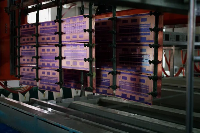
Image scope: the photographs below are licensed representative process images, not claims that the pictured people or equipment belong to PCBA PARTNER. Project-specific factory, fixture, inspection, and release evidence can be provided during RFQ review when available.
1. Project kickoff and engineering review
After receiving Gerber files, BOM, assembly drawings, and process requirements, our engineers run DFM/DFA review: pad design, component spacing, test points, panelization, stencil openings, and reflow profile feasibility. Issues caught here often determine whether you later see bridges, tombstoning, or insufficient solder.
2. Materials and supply chain
- Consignment or turnkey procurement with MPN, package, and MSL verification
- Lifecycle and lead-time review for critical ICs and connectors
- Incoming IQC: visual, marking, and X-Ray sampling by risk level
3. Solder paste printing and SPI
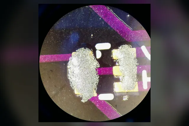
Stencil design, paste condition, print alignment, and SPI feedback create the foundation for stable SMT yield. Paste deposits should be evaluated by aperture, component geometry, and first-article results instead of by a single generic threshold.




4. SMT placement and reflow
Placement programs, feeders, nozzle selection, first-article verification, and a validated thermal profile form the SMT backbone. Fine-pitch QFN/BGA and small passive components require tighter setup and inspection planning.


5. THT, wave soldering, and manual operations
Mixed-technology assemblies may add through-hole insertion, selective or wave soldering, hand soldering, cleaning, and controlled rework. Criteria should define acceptable fill, wetting, residue, workmanship, and re-inspection.


6. ICT, functional test, and release
Test coverage should be defined before fixture release. ICT, flying probe, functional checks, programming, burn-in, and cosmetic inspection are selected according to product risk, access, volume, and customer acceptance requirements.


After test and outgoing inspection, boards are packed and shipped with the agreed evidence. Deliverables can include COA, inspection summaries, test reports, reflow profiles, programming records, and release photographs. PCBA PARTNER scales the evidence package by project stage—EVT, DVT, PVT, or repeat production.
For a build-lot summary, see the PCBA production yield report template, which separates first-pass yield, rework, and logged defect occurrences.
Representative image credits and licenses
Images were cropped, color-balanced, and converted to WebP for this page. Pexels photographs are used under the Pexels License. Wikimedia Commons credits:
- Solder printing machine — Nelatan, public domain.
- Solder paste inspection machine — Nelatan, CC BY-SA 3.0.
- Solder paste macro — Autopilot, CC BY-SA 3.0.
- Solderpaste image series 1–9 — oskay, CC BY 2.0.
- Pick-and-place machine interior — Peripitus, CC BY-SA 3.0.
- Placement head control boards — Ossewa, CC BY 4.0.
- Juki KE-2080L — Megger Ltd., CC BY 3.0.
- Reflow oven — Nelatan, CC BY-SA 3.0.
- Selective soldering nozzles — Pedro ximenez, CC BY-SA 3.0.
- THT assembly — ECD Electronic Components GmbH Dresden, CC BY-SA 3.0.
- PCB electroplating line — Swoolverton, CC BY-SA 3.0.
Planning a new program? Contact our China PCBA manufacturing team for a manufacturability review and lead-time estimate.