Two lighting channels
The design uses five common-anode dual-color LED placeholders with separate white and warm channels. Each LED color has its own current-limiting resistor. The final LED package and pin order remain to be confirmed.
CULTURAL LIGHTING · ENGINEERING FILES
A compact lighting board shaped around the product: five dual-color LEDs, touch input and USB-C charging in a 50 mm C-shaped layout. Explore the supplied reference hardware and the editable KiCad design.
Project identified by the material provider as a Palace Museum cultural lamp. This page presents supplied hardware photographs and an engineering candidate.
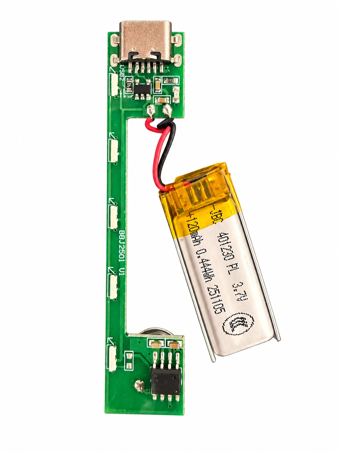
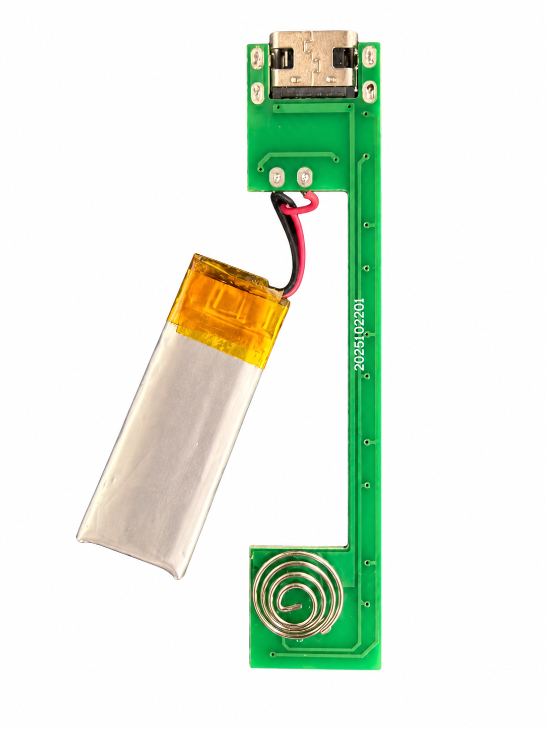
The two photographs show the supplied lamp electronics with a connected pouch battery. The white background was edited from the original photographs. These images document the reference hardware; they do not establish that the V0.5 CAD candidate has been assembled or tested.
The design uses five common-anode dual-color LED placeholders with separate white and warm channels. Each LED color has its own current-limiting resistor. The final LED package and pin order remain to be confirmed.
Planned sequence: white → warm → off, with a spring touch electrode. Firmware, touch-library integration and enclosure sensitivity tuning remain pending.
The candidate combines USB input, a single-cell lithium charging circuit and a USB-priority power path. The engineering notes specify a nominal 3.7 V / 120 mAh protected battery and an initial charging target of about 30 mA, subject to cell and bench verification.
V0.5 contains 55 footprints, 412 track segments and 35 through vias. The supplied 3D views include placeholder LED, USB and touch-spring models. Board width, component fit and enclosure clearances require physical confirmation.
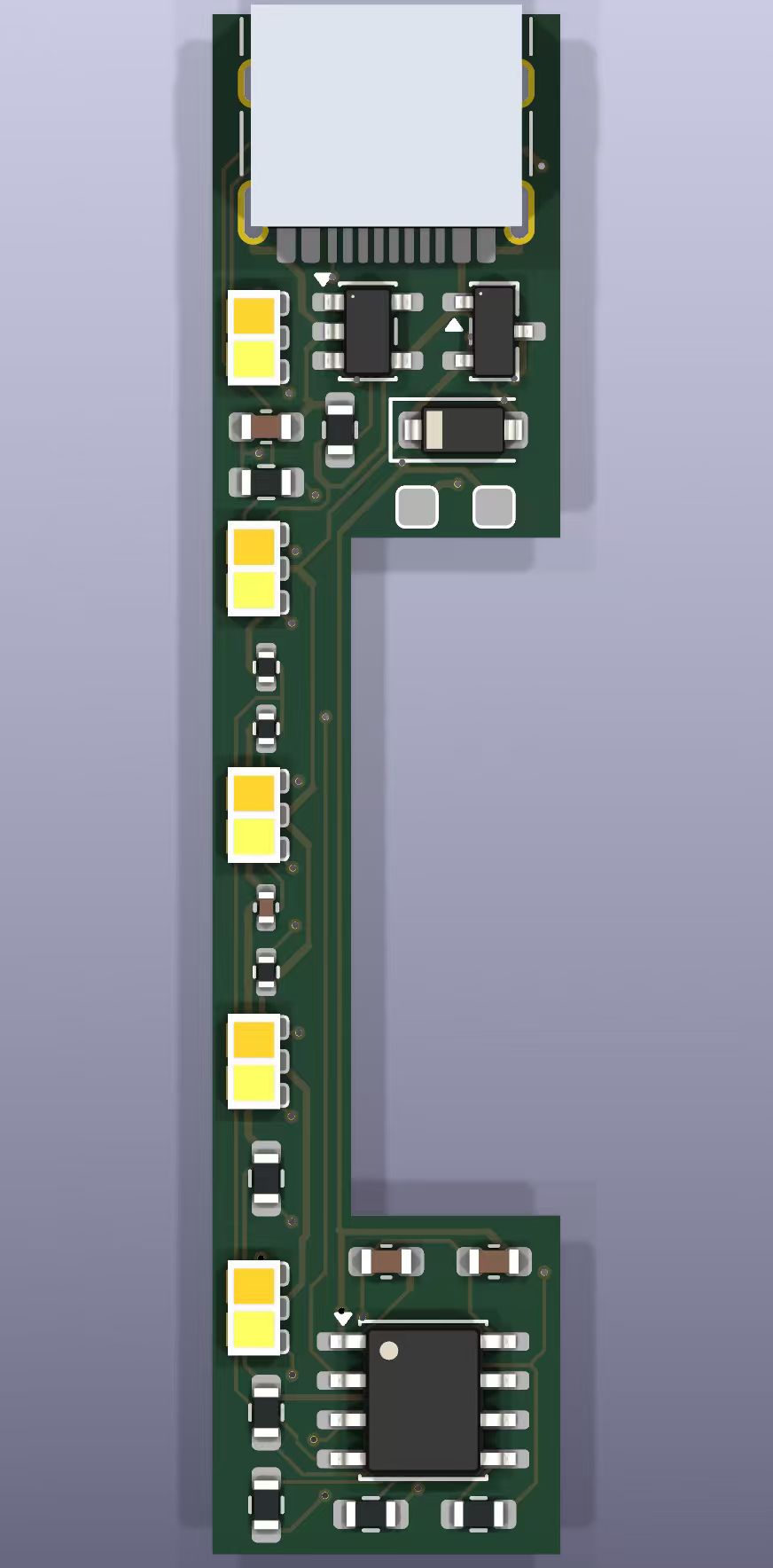
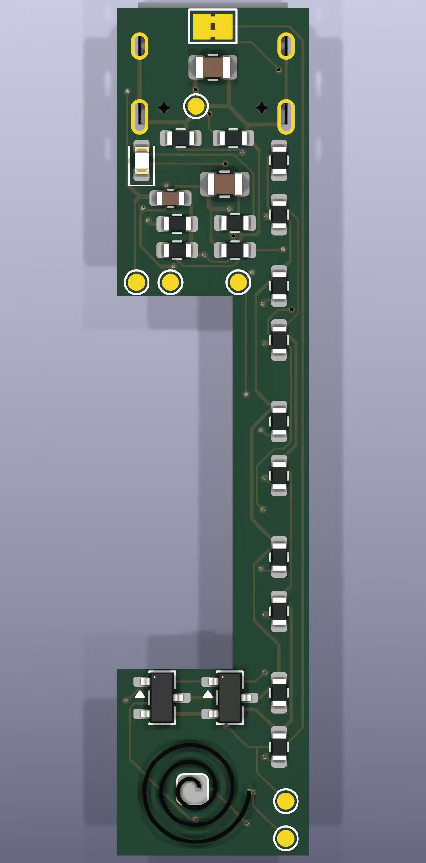
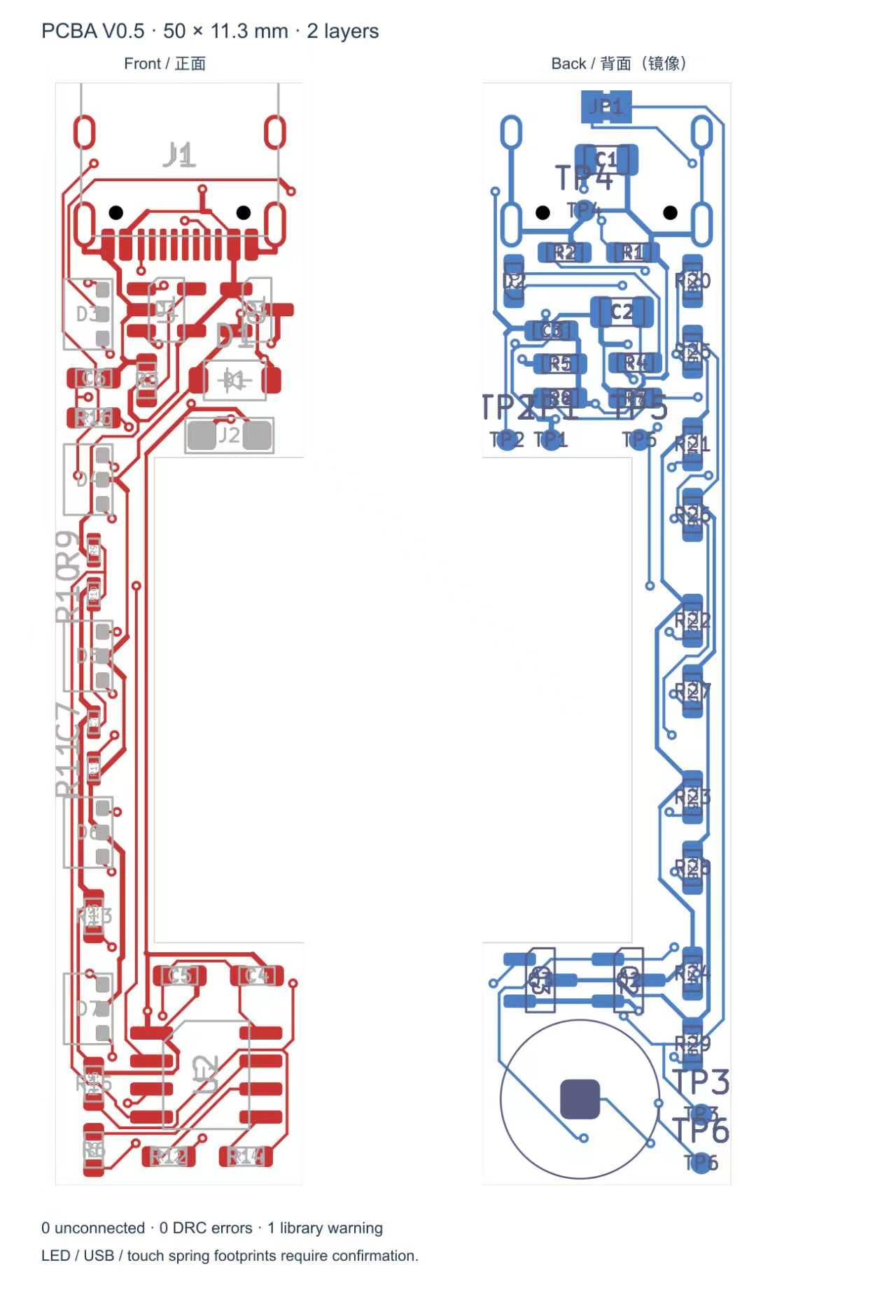
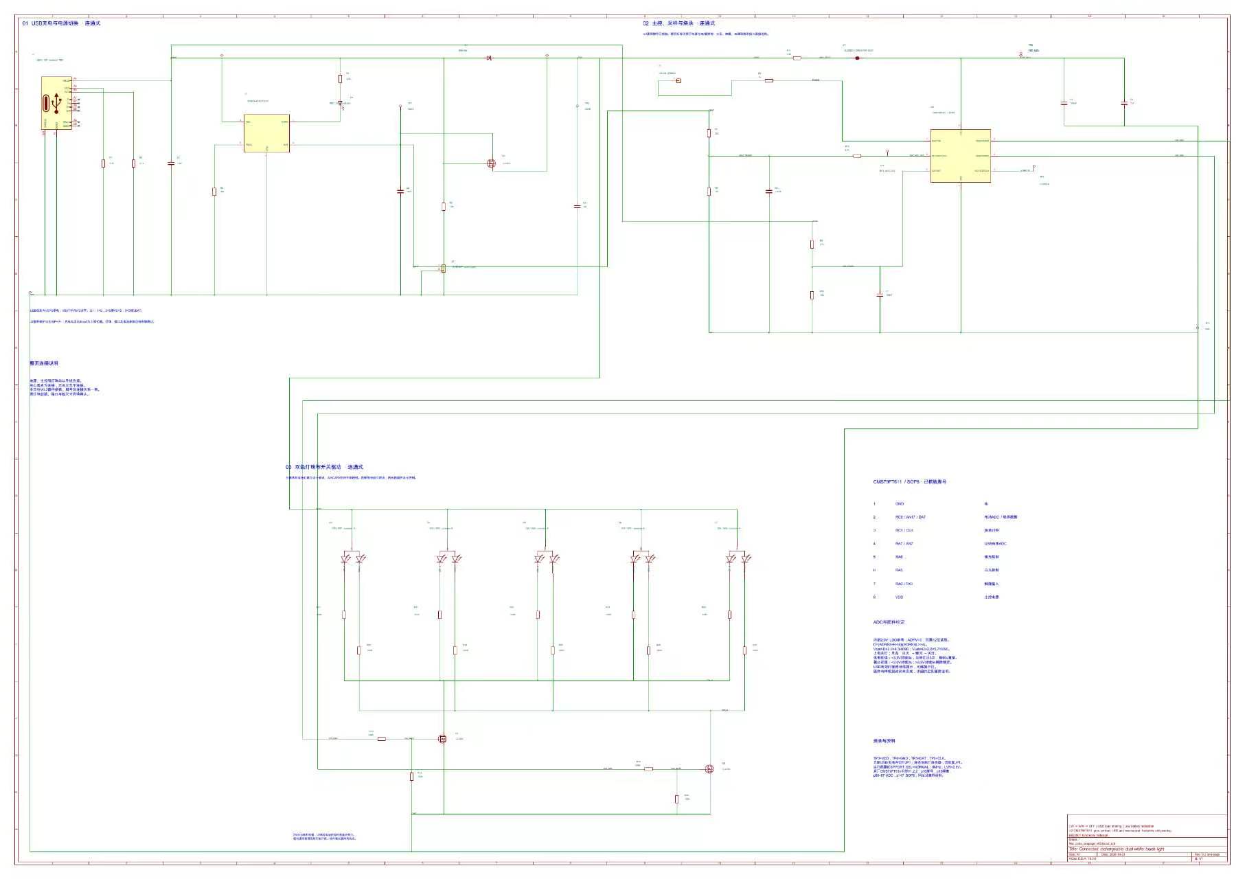
The figures below are taken from the supplied engineering records, dated 23 October 2026. They were not rerun for this website publication.
| PCB connectivity | 0 unconnected items in the supplied report |
|---|---|
| Design rule check | 0 errors; 1 USB footprint-library mismatch warning |
| Schematic check | No violations reported; inspect the ERC JSON for configured checks |
| Firmware | Not implemented, compiled or programmed in these packages |
| Prototype validation | V0.5 assembly, touch, charging, thermal and optical tests pending |
| Manufacturing files | No production Gerber release included |
Before a build: confirm the LED polarity and pad numbering, USB connector and touch-spring dimensions, battery protection and charging conditions, and the final enclosure fit.
Original ZIP archives are preserved byte for byte. V0.5 is the current routed PCB package; V0.3 retains the earlier single-page schematic and its V0.2 reference BOM.
Share the enclosure space, desired lighting, touch behavior, battery requirements and target quantity to define the engineering and prototype scope.
Discuss your project ↗