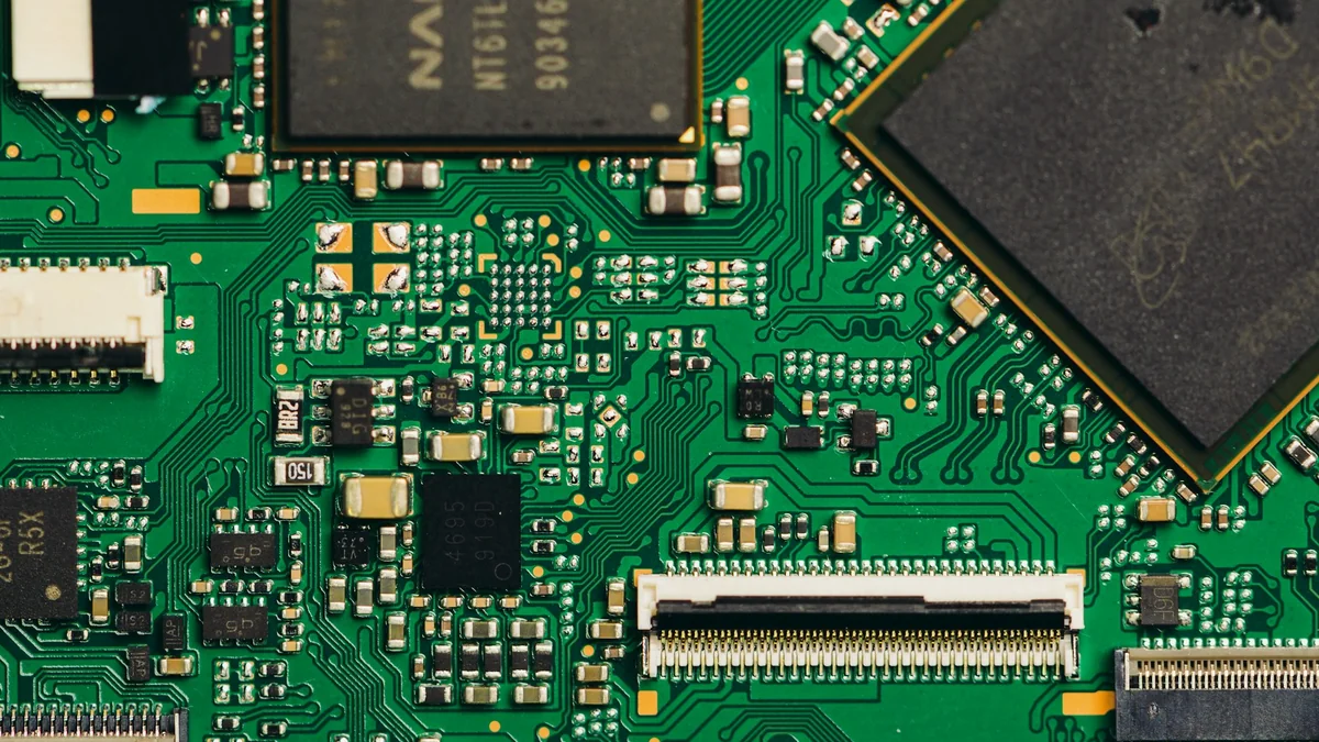
A PCB can look correct in the layout editor and still arrive at the factory as an incomplete manufacturing package. The export is a separate deliverable: a missing internal layer, an old drill file, or an ambiguous outline can change what the supplier understands. Before sending Gerber files for PCB assembly, review the files the supplier will receive, not only the design that produced them.
The workflow below focuses on that handoff. For the wider quotation package, see our PCB assembly quote package checklist.
1. Export from one approved design state
Save the board and resolve outstanding design-rule findings before generating outputs. Export into a new, empty folder named for the board and revision. Reusing a previous output directory makes it easy to leave an obsolete file beside a newly generated one, particularly when a layer or hole type has been removed.
Keep the export configuration with the design. Altium's Output Job files, for example, store settings for output types, naming, formats, and locations. A saved configuration makes the next export reproducible; it does not prove the selected board or revision is correct. Check those inputs before running it. Altium's output and release documentation explains this distinction in the workflow.
2. Make every layer's purpose clear
Inventory the copper layers in physical order, then the required top and bottom solder mask and silkscreen. Include paste outputs for the sides to be assembled when the agreed package requires them. Keep assembly drawings and fabrication notes identifiable as documentation rather than mixing their graphics into copper images.
When supported by the receiving workflow, export Gerber X2 attributes. They carry information about a file's function and objects that would otherwise require interpretation. Clear filenames remain useful for people reviewing the archive, but renaming a file cannot repair incorrect content. Ucamco's explanation of Gerber X2 describes the role of these attributes.
Inspect export settings that alter the output. In KiCad, deselected layers are omitted; plotting the drawing sheet adds its border and title block; and the zone-fill check helps avoid outdated fill geometry. These are examples of why the saved board's appearance and the exported files can differ. Consult the instructions for your EDA version rather than copying an old dialog screenshot. KiCad's plotting documentation details these controls.
3. Define the board edge as manufacturing data
Provide a separate profile file with an accurately connected closed boundary. Under the current Gerber specification, the profile can be represented by a contour or a closed path of lines and arcs; when a nonzero-width path is used, its centerline defines the edge. The profile can also include cutout openings. A dimensioned drawing helps explain intent, but it does not replace this machine-readable geometry. Ucamco's Gerber specification, section 6.5 defines these requirements.
Check the exported overall dimensions against the mechanical design. Look for disconnected corners, duplicate edges, construction lines, and a second outline that could be mistaken for a panel boundary. If panelization is required, explicitly identify whether the package describes one board or an approved panel.
4. Check holes and slots separately
Generate the actual drill and routing outputs, not just a drill map. Identify plated and non-plated holes and any special layer spans. Inspect slotted connector holes as slots: a copper pad with an oval shape is not evidence that its opening was exported correctly.
EDA tools offer different drill-output controls. Altium documents separate plated/non-plated outputs, separate hole-shape files, layer-pair outputs, and optional board-edge routing data. Its guidance also calls for compatible coordinate formats and the same origin reference as the Gerber output. Agree the accepted drill format with the supplier, then check all resulting files together. Altium's fabrication-data documentation covers these settings.
Flag critical finished-hole dimensions and tolerances in the fabrication requirements. If both profile and routing data describe an opening, reconcile any difference before release.
5. Open the exact archive in an independent viewer
Close the design editor's preview and open the generated files as a manufacturing dataset. Copper, mask, profile, and drill data should align without manually dragging layers into place. Keep a common origin and axis orientation; do not mirror bottom fabrication layers simply to make their text readable. Ucamco's fabrication-data guide, section 5 explains why registration must be preserved.
Use an approved local or browser viewer for confidential designs. Our Gerber viewer and Gerber layer checks can support the review. Inspect each layer individually, then overlay copper with holes and mask openings. Check a known dimension, fine-pitch pads, mounting holes, connector slots, and edge features. Visual review complements the supplier's CAM and manufacturability checks.
6. Release one package with a clear status
Zip the reviewed folder and open that ZIP once more. Add a brief manifest with the board identifier, revision, copper-layer order, file purposes, and unresolved questions. State whether it is for quotation, engineering review, or production release. When a change is necessary, regenerate the affected dataset and issue a new package instead of emailing a loose replacement layer.
Gerber fabrication files do not replace the BOM, component placement list (CPL), assembly instructions, or test requirements. Keep those deliverables consistent with the same approved design state; our PCBA release and revision-control guide covers their coordination. Submit the reviewed package through the PCBA RFQ page, and resolve any supplier questions against that identified revision before authorizing manufacture.