12 V INPUTFuse + reverse-polarity protectionSMBJ15A transient suppression
PROTECTED BUSMotor and auxiliary branchesSwitched LED / UV outputs
LOGIC SUPPLY2 × TPS54302 buck stagesLocal control and sensor domains
Open hardware · Smart pet electronics
An A1 control-board design combining motor drive, precision weighing, sensor interlocks and Wi-Fi connectivity. Explore the circuit architecture, engineering decisions and editable KiCad source.
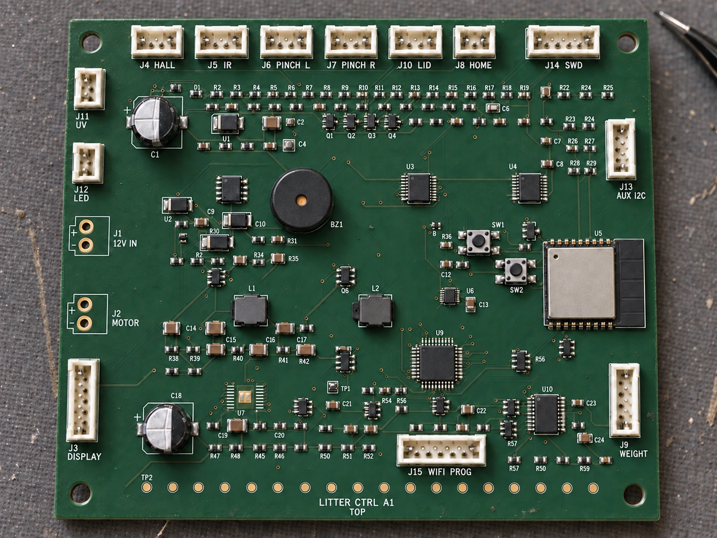
01 / Control architecture
The design separates motor power, low-level weighing signals, local control and wireless communication. Eleven hierarchical schematic sheets keep the power, sensing and interlock paths traceable.
STM32G0 drive commands go to the H-bridge; current-sense and fault signals return to the local controller.
A1 / ENGINEERING VIEWS
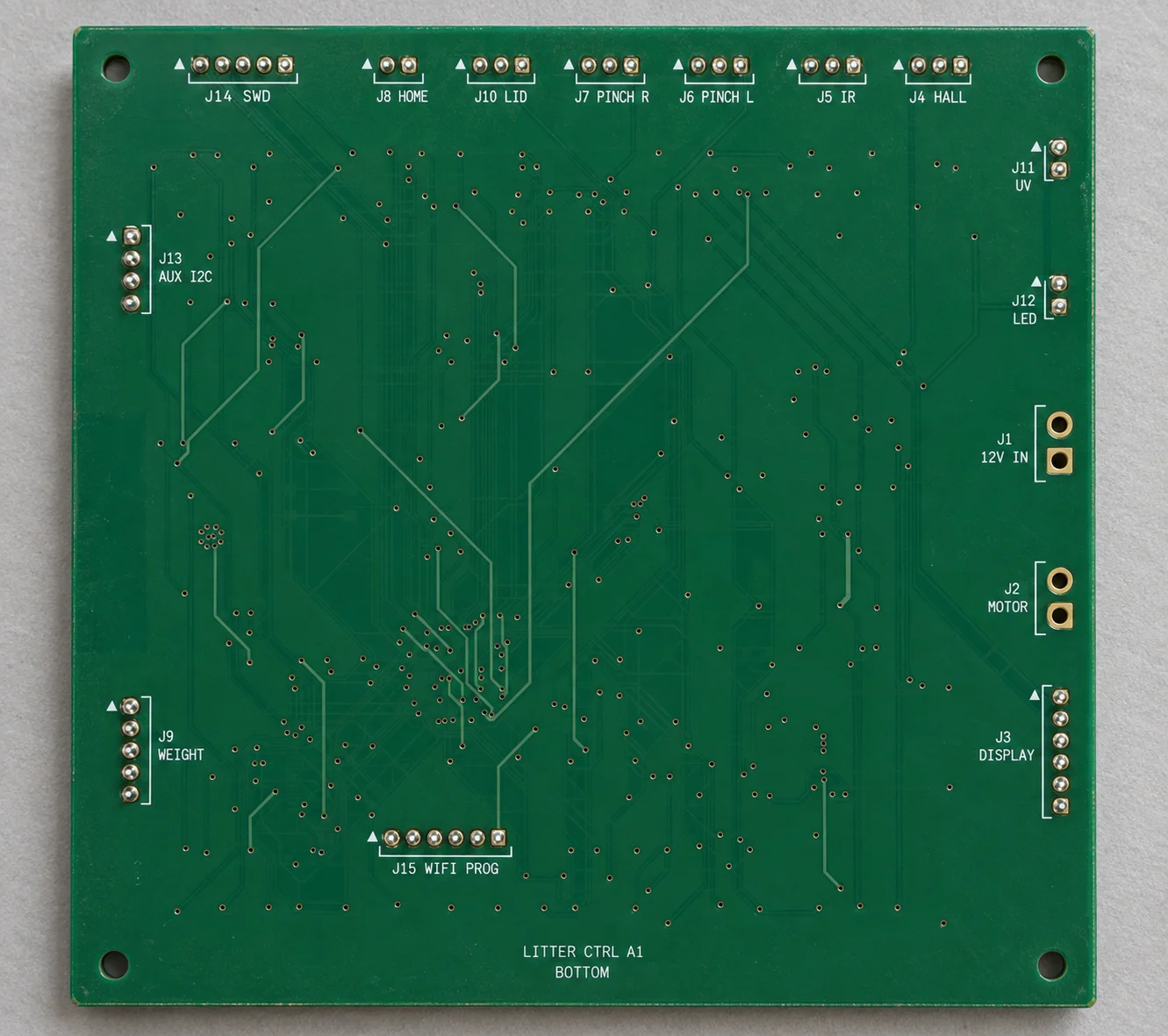
Source-derived previews show how the 12 V motor path and low-level weighing front end connect to the routed PCB.
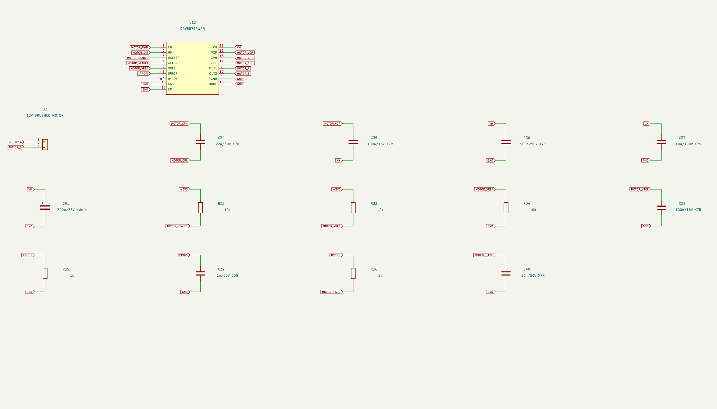
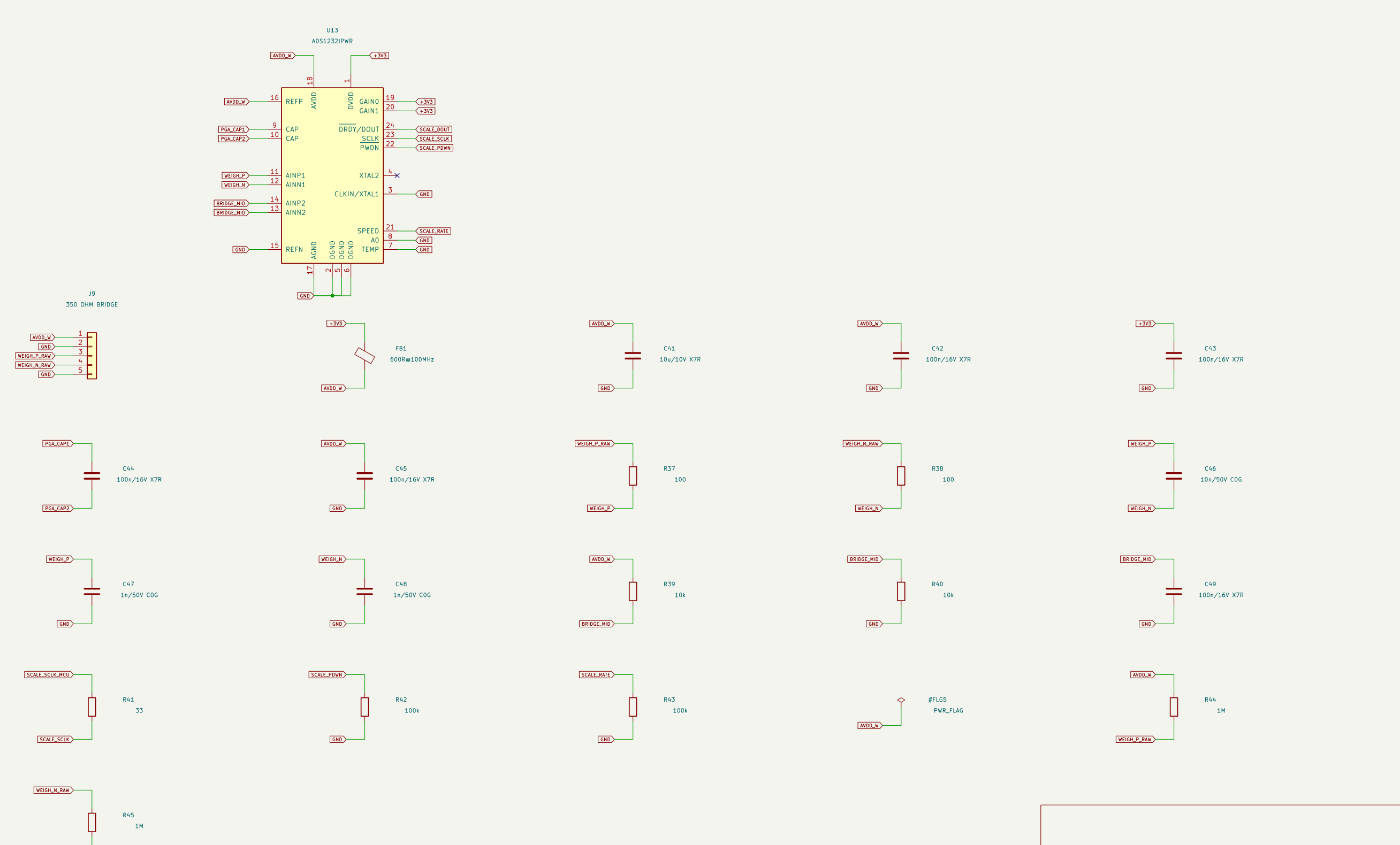
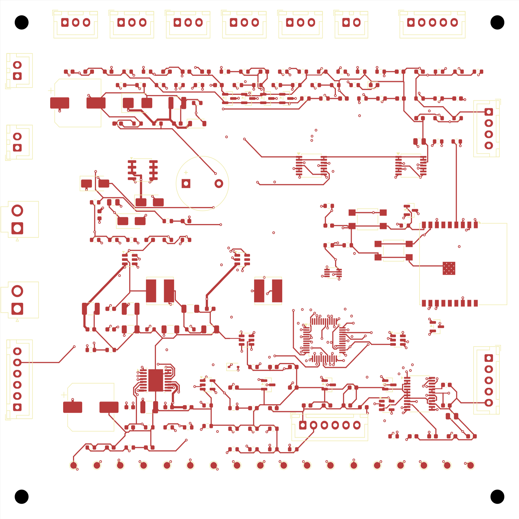
A 3 A fuse selection, AO4407A reverse-polarity stage and SMBJ15A transient suppressor form the input network. Two TPS54302 buck stages supply the logic domains. Inrush, motor regeneration and fuse coordination drive the protection review.
The STM32G030C8T6 handles the local control interface, with a TPS3839 supply supervisor. An ESP32-C3-WROOM-02-N4 module provides the wireless interface. Separate SWD and Wi-Fi programming connections support board bring-up and firmware access.
A DRV8876 H-bridge connects to the brushed DC motor. Its current-sense feedback and fault signals give the control architecture inputs for load monitoring and fault handling. Motor current, reversal energy and driver dissipation determine the operating envelope.
The ADS1232 24-bit ADC interfaces with the nominal 350 Ω bridge connection. Input filtering, reference routing, ground return and calibration must preserve a small differential signal beside a switching motor and a radio module.
Hall, home, lid, infrared and left/right pinch channels are defined separately. TLV1704 comparator stages and SN74LVC logic form the window-detection and hardware-interlock path. Thresholds, cable faults and reset behavior require coordinated hardware and firmware rules.
The display header provides a 5 V supply with 3.3 V UART logic; the auxiliary I²C header uses 3.3 V logic. Switched 12 V LED and optional UV outputs have a 0.2 A design limit per channel. Optional UV operation needs a defined enclosure and interlock requirement.
| Connector | Function | Key interface details |
|---|---|---|
| J1 / J2 | 12 V input / motor | J1: VIN_RAW, GND · J2: MOTOR_A, MOTOR_B · JST-VH 3.96 mm family |
| J3 | Display / controls | 6-pin header; +5 V supply, 3.3 V UART logic, reset and user-key signals |
| J4 / J5 | Hall / IR | Separate 3-pin inputs with +5 V, GND and a dedicated sensor signal |
| J6 / J7 / J8 / J10 | Pinch / home / lid | Dedicated left/right pinch, home-contact and lid-interlock signals; full pin order in CSV |
| J9 | Weight bridge | 5-pin nominal 350 Ω bridge connection to the ADS1232 front end |
| J11 / J12 | UV / LED outputs | Switched 12 V outputs with a 0.2 A design limit per channel |
| J13 / J14 / J15 | Aux I²C / SWD / Wi-Fi programming | 3.3 V logic and reference connections; consult the pin-level CSV before wiring |
Signal names follow the A1 schematic. Check the connector orientation, mating part and harness polarity against the target appliance before wiring.
02 / Engineering difficulty
Component selection is only one part of the design. The main challenges are the interactions between motion, measurement, interlocks and the mechanical assembly.
Stall, start-up, braking and reversal produce different electrical stresses. The driver, bulk capacitance, TVS, fuse and copper paths need one consistent current and energy budget. The routing audit records 0.5 mm motor-output traces and local motor-bus neckdowns of about 0.375–0.401 mm; current and temperature limits must be assessed with the selected motor.
Motor PWM, regulator switching and wireless activity can disturb bridge measurements. The design review therefore considers analog return paths, input symmetry, reference decoupling and measurement timing. Zero tracking, load calibration and filtering belong in the complete weighing strategy.
A useful interlock specification covers more than a normal sensor reading: open cables, short circuits, reset, brownout, a stuck input and communication loss all need defined states. Hardware gating, MCU commands and fault recovery must agree on when motion is permitted and how it is stopped.
The A1 outline is 120 × 116 mm, with four mounting holes and a 1.6 mm, four-layer stack-up. Board-edge clearances, connector keying, cable exits, component height and the antenna environment all affect integration. The source makes these design choices inspectable for adaptation to a specific enclosure.
03 / Open design package
The package includes editable KiCad 10 schematics and PCB source, a schematic PDF, a component BOM, connector definitions and machine-readable design audits.
These records contain the KiCad checks behind the figures above. Electrical ratings, dimensional requirements and acceptance limits are set for the target appliance. Component references: DRV8876, ADS1232, TPS54302.
04 / Product application
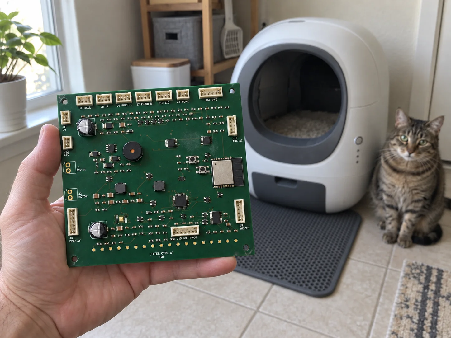
The enclosure, rotating mechanism, sensor placement and service access define the controller requirements. Share those interfaces early so the electrical design and mechanical assembly can be reviewed together.
05 / Open hardware
The original hardware design source is shared under the permissive CERN Open Hardware Licence Version 2. Commercial use and modification are allowed under its terms and notice requirements. The download contains the full licence; see the official licence text.
Tell us about your controller project
Share the product functions, supply and motor requirements, sensor types, board dimensions and expected quantity. Attach existing files or start with a short technical brief.
Files are optional to start. This project reference is included in the inquiry link.