Cellular and GNSS paths
SIM7080G forms the cellular/GNSS architecture, with separate LTE and GNSS antenna connections. Module and antenna selection can be scoped around your target region, operator and enclosure.
Pet tracker PCBA · PET-TRACKER-V05
A 45 × 35 mm PCBA design combining cellular connectivity, a GNSS interface, motion sensing and single-cell battery power. Explore the component layout, connectivity architecture and assembly choices for a compact wearable device.
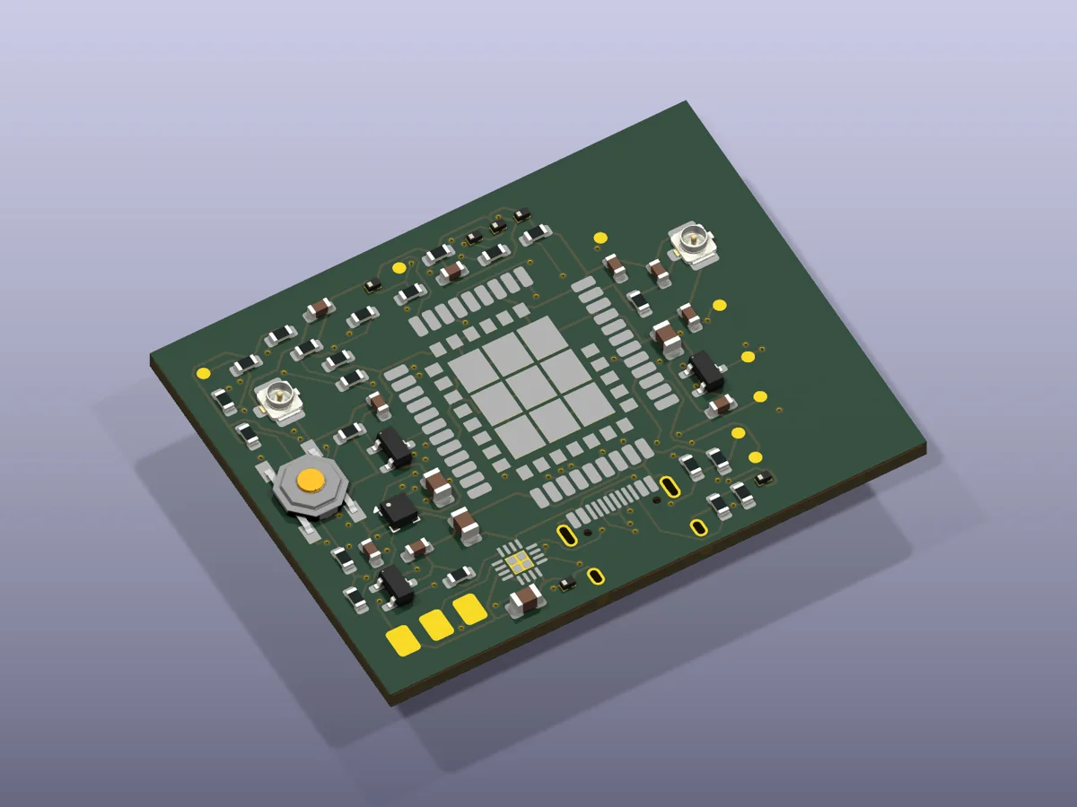
01 / System architecture
The design combines cellular and GNSS connectivity with a local controller, motion sensor, Hall-sensor input and single-cell battery power.
SIM7080G forms the cellular/GNSS architecture, with separate LTE and GNSS antenna connections. Module and antenna selection can be scoped around your target region, operator and enclosure.
STM32L031K6U6 provides local control, paired with an LIS2DW12 motion sensor. This hardware combination provides inputs for movement-aware sleep and reporting logic.
BQ24074 provides charging and power-path management for a single-cell Li-ion battery. Battery capacity, charging input and reporting frequency are key inputs to the device power budget.
DRV5032 provides a Hall-sensor input for magnetic attachment sensing. The interface can be used with a magnet in the collar bracket to detect a change in attachment state.
02 / Size and cost
The board measures 45 × 35 mm, with a total area of 1,575 mm². Cost planning covers the PCB, components, assembly, battery, antennas and final enclosure.
The 1.6 mm PCB uses four copper layers and through vias. The design avoids blind and buried vias, with a 45 × 35 mm outline for a compact electronics package.
The layout places 59 footprints on top and 23 underneath. Using both sides reduces the space needed on one face of the board; assembly cost also depends on the component mix and process sequence.
The modem, controller, sensors, charging IC and connectors define the main sourcing requirements. A quotation can include agreed manufacturer part numbers, component grades and substitution rules.
Compare quotations at the same order quantity and scope. Include the PCB stack-up, components, double-sided assembly, inspection, programming, fixtures and final-device assembly.
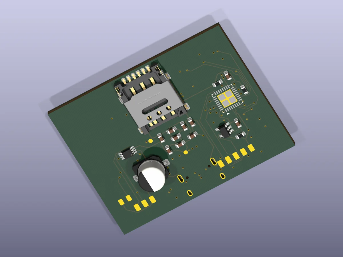
03 / Board layout
The board brings radio, sensing and power interfaces into a double-sided layout. Separate antenna connections and dedicated battery and debug pads support device integration.
04 / Hardware detail
Dedicated interfaces separate the cellular module, local controller, sensors and charging circuit. The component choices below describe the board architecture.
The STM32L031K6U6 communicates with the SIM7080G over UART through a TXU0202 interface buffer. Separate modem power-key and DTR control signals give firmware control over startup and sleep requests.
The LIS2DW12 connects over I²C and provides an interrupt line to the controller. The DRV5032 Hall sensor provides a separate magnetic input. Firmware can use these inputs to change the reporting schedule or recognize a collar-bracket state change.
| Circuit | Component / connection | Role in the device |
|---|---|---|
| Cellular / GNSS | SIM7080G module architecture | LTE-M / NB-IoT connectivity; select the module order code and GNSS option for the target network and application. |
| Local control | STM32L031K6U6 | Sensor sampling, modem control and application timing. |
| Motion sensing | LIS2DW12 · I²C + interrupt | Three-axis acceleration input for movement-aware operation. |
| Magnetic sensing | DRV5032FADBZR | Magnet detection at the collar attachment; bracket geometry defines the switching position. |
| Charging | BQ24074RGTR | Single-cell Li-ion charging and system power-path management. |
| Logic supply | TLV70018DDCR | 1.8 V regulator for the logic rail. |
Component references: SIMCom SIM7080G · ST LIS2DW12 · TI TXU0202
05 / Power architecture
USB input feeds the charger and system rail. The battery supports the device away from USB and can supplement the system load during radio activity.
The BQ24074 EN1 and EN2 pins are tied low, selecting the 100 mA maximum input-current mode. The 8.87 kΩ ISET resistor corresponds to approximately 100 mA nominal programmed charging current. System demand, input limiting and temperature can reduce the current reaching the battery.
J2 uses VBAT, BAT_NTC and GND pads for a single-cell battery pack with temperature sensing. Specify pack protection, NTC characteristic, cable resistance and pulse-current capability together with the available battery envelope.
The modem supply path is VSYS → R7 → VMODEM. Local capacitance is specified as 100 µF polymer, 22 µF ceramic and 100 nF decoupling. Capacitor ESR, ceramic capacitance under bias and total path resistance determine the supply response during a transmit burst.
Battery sizing depends on the time spent asleep, acquiring a location, registering on the network and uploading data. Estimate daily energy from each mode’s current and duration, including retries and low-signal operation; use this profile to choose capacity and reporting intervals.
Charge-current values describe the resistor setting, not a charge-time guarantee. Power-path and input-mode reference: TI BQ24074 datasheet.
06 / Integration interfaces
Connector height, cable bends and fixture access all contribute to the finished device envelope around the 45 × 35 mm board.
| Interface | Board connection | Integration detail |
|---|---|---|
| USB-C · J1 | 5 V input and modem USB data | Allow cable access and connector support. Higher-current charging requires source-capability detection and a controlled input-current setting. |
| LTE antenna · J3 | U.FL coaxial connector | Select an antenna for the operator’s bands and reserve cable routing and antenna clearance. |
| GNSS antenna · J4 | Separate U.FL connector | The connection is for a passive GNSS antenna; an active antenna needs a suitable bias supply. |
| Subscriber identity · J5 | 1.8 V nanoSIM interface | Specify a compatible SIM and operator profile; account for holder access during assembly. |
| Programming / debug | 1.8 V SWD and UART pogo pads | Use a 1.8 V-compatible programming/debug adapter. Provide fixture clearance, a ground reference and a programming sequence. |
| Battery · J2 | VBAT / BAT_NTC / GND solder pads | Include strain relief and polarity control for the battery harness. |
LTE and GNSS have separate feed paths and matching-component positions. Specify feed geometry against the fabricator’s stack-up, then tune the antenna system with the battery, enclosure and collar hardware in place. Keep conductive hardware away from the antenna’s required clearance region.
Allow space above and below the PCB for components, the battery, antenna connectors and cable bends. Locate the bracket magnet relative to the Hall sensor and define retention, seal geometry and USB access as part of the housing design.
07 / Application behavior
Firmware and cloud scope can be specified around four operating scenarios. Reporting intervals, event thresholds and data retention are product choices.
Use the motion interrupt to wake local processing. Combine a periodic heartbeat with inactivity timing; coordinate modem sleep requests with the operator’s supported network behavior.
Set a location-acquisition timeout, timestamp every fix and define an active reporting interval. A phone interface should distinguish a recent fix from the last known position.
Apply debounce and persistence thresholds to the Hall-sensor signal before creating an event. Define how the product handles magnet alignment, vibration and intentional removal.
Specify retry backoff and a bounded queue for timestamped records. Storage capacity and write endurance determine how much history can be retained. Geofence alerts also need a defined device-to-cloud and cloud-to-phone delivery path.
08 / Assembly and cost
A useful quotation separates recurring board cost from tooling, programming and final-device integration.
Four copper layers, a 1.6 mm board and through vias define the fabrication scope. Double-sided placement saves face area but adds handling and process considerations for the assembly supplier.
Keep RF matching options and unpopulated positions explicit in the BOM. Compare the modem, antenna, battery and connectors by exact specification; quote alternatives with their electrical and mechanical differences listed.
Separate fixture and programming setup from per-unit charges. Define inspection access for QFN/LGA packages, battery connection, radio checks, serialization and whether the scope ends at the PCBA or includes the complete device.
Build around your tracking requirements
Share your target market and operator, battery envelope, reporting interval, collar attachment and expected quantity. These inputs define the antenna space, power budget and assembly scope.
Files are optional to start. The inquiry link includes project reference PET-TRACKER-V05.